First Steps
First things first, as much as I want to jump straight into coding away, I need to have a proper analysis of how the different parts of the Game Boy Color work. To better understand the hardware components, I’ll be using the Game Boy PanDocs document, widely regarded as the most comprehensive public technical reference for the Game Boy.
Overview
In order to plan out the emulator, it’s important to know what components and functions make up the console.
Inside of a Game Boy Color, there are a couple different processors that I will need to emulate to get games to work:
- An 8 bit Sharp SM83 CPU for the main processor
- A Picture Processing Unit (PPU) capable of rendering a max of 10 sprites per line, or 40 sprites to the screen in 32 768 different colours
- An Audio Processing Unit (APU) to provide audio through 4 channels with stereo output
I’ll also need to handle user input, which will not only involve reading the input from the keyboard, but also emulating I/O related hardware interrupts.
The CPU
The Game Boy Color used the same Sharp SM83 CPU as the original Game Boy, with the exception that it’s clock speed was now roughly 8.38 MHz — double the clock speed of the original. In order to keep the console backwards compatible with the original Game Boy’s games, the Game Boy Color’s CPU had 2 modes: Normal mode with a clock speed of roughly 4.19 MHz; and Dual-speed mode with the aforementioned speed of ~8.38MHz.
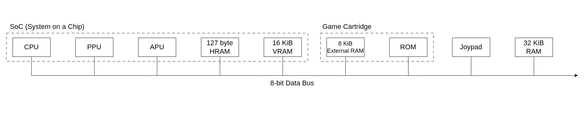
The Sharp SM83 had an addressable memory space of 64 KiB with it’s 16-bit address bus, and is used for ROM, RAM, and I/O. Connecting all these together was an 8-bit data bus.
Additionally, there was also 32 KiB of memory stored onboard of the motherboard.
The PPU
To render graphics to the screen, the Game Boy Color would use it’s PPU, which is capable of rendering a max of 10 sprites per line, or 40 sprites to the screen in 32 768 different colours. An interesting detail here though, is that the PPU is only responsible for rendering the images to the screen, all graphics-related calculations are actually done by the CPU.
To generate images, the Game Boy uses 8x8px squares called tiles as the base unit, and 4 arrays of colours which form a palette.
Graphics are rendered in 3 different layers: Background; Window which is used UI elements like health bars; and Objects which can move independently and are combined to create sprites.
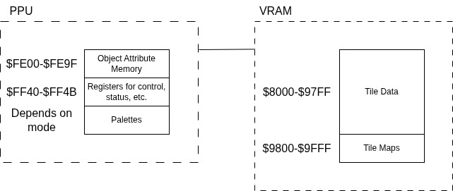
To store tile-related data, the PPU is connected to 8 KiB VRAM on the motherboard, while other data such as Palettes and Objects are stored in it’s own address space.
The APU
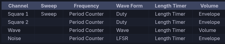
The APU provides four audio channels to play sound.
 From Game Boy PanDocs
These are controlled by writing to specific registers, located in registers $FF10-$FF26.
There are a lot of complicated functions to each of these that I haven’t gone over in this entry, but those will be discussed in depth in future posts when I share insights on various implementations of these components.
Initial Software Architecture
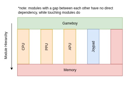 This leaves us with the above architecture.
I’ve designed this so that the Gameboy module will act as a sort of Control class, containing all of the other modules and orchestrating their operation.
Each of the components will exist independent to each other, with no direct dependency to another component aside from memory. This way, one module cannot directly interact with or modify another, and must rely on passing data to memory for another module to pick up, resulting in a much safer design. I’ve also grouped all memory regions into a singular Memory module to keep things clean.
Keep in mind that this is only an initial design, and is subject to change as complexities arise over the course of development.